When shopping for a new graphics card, there are a number of factors to consider; memory is among the most notable and crucial.
While GDDR5 memory was widely used by GPUs over the past decade, both AMD and Nvidia have since migrated to GDDR6. Both of these are commonly used in modern GPUs, but they are hardly the only options.
Bạn đang xem: Hbm Hbm2 Hbm2e Update 07/2026
HBM, along with its successors HBM2 and HBM2E, is a new technology that is rarely seen in current-generation graphics processing units (GPUs).
Therefore, please explain HBM, HBM2, and HBM2E. How are they different from one another and from GDDR memory? Is it true that GPUs with HBM are superior for gaming? Find the details in the following section.
What Is HBM?
As was mentioned up top, some modern graphics cards make use of HBM, a form of SDRAM (synchronous dynamic random-access memory) comparable to GDDR. Since HBM is an acronym for “High Bandwidth Memory,” its very name gives away its defining feature: its bandwidth. Of course, that’s not all the benefits it provides.
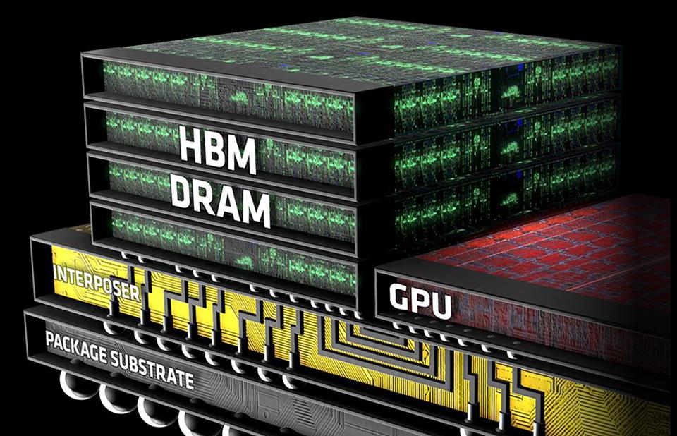
Since multiple memory dies are “stacked” on top of one another, HBM not only has significantly greater bandwidth than DDR or GDDR memory, but it also consumes less power and takes up less space on the PCB.
![What Are HBM, HBM2 and HBM2E? [Ultimate Guide] - YouTube](https://gemaga.com/wp-content/uploads/2023/04/hbm-hbm2-hbm2e-1.jpg)
Each HBM die has a memory bus of 1024 bits and a bandwidth of 128 GB/s; when stacked, these values increase to 4096 bits, 512 GB/s, and 4 GB/s, respectively. Needless to say, these specifications are light years ahead of the previous standard, GDDR5, especially considering the introduction of the first GPUs with HBM in 2015.
Few AMD GPUs shipped with HBM memory, however; these included the Radeon R9 Fury, Radeon R9 Nano, Radeon R9 Fury X, and the Radeon Pro Duo. It wasn’t until HBM2 came along that it was used on a larger scale.
What Is HBM2?
Now we’ve arrived at HBM2, the second generation of High Bandwidth Memory, which vastly improved upon the key features of its predecessor by providing twice the bandwidth (256 GB/s) per die, supporting up to 8 GB of memory on a single die, and permitting 8-die stacks, greatly increasing the overall performance potential of HBM2.
As was previously mentioned, HBM2 has been incorporated into a growing number of GPUs over the years, including the Radeon RX Vega series, the Radeon VII, and a number of Radeon Pro GPUs from both AMD and Nvidia, as well as a few of Nvidia’s workstation-oriented GPUs, including the Titan V and the Quadro GP100.
What Is HBM2E?
Then there’s HBM2E, the newest version of High Bandwidth Memory. With a maximum stack size of 12 dies and an increase in maximum memory per stack to a massive 24 GB, it was first announced by JEDEC in 2018. It supports a bandwidth of up to 307 GB/s per die.
Companies like Samsung and SK Hynix have since announced their own HBM2E iterations. Both allow for memory and die stacks of up to 16 GB, and die stacks of up to 8 dies. The HBM2E from Samsung provides 410 GB/s of bandwidth, while the HBM2E from SK Hynix provides 460 GB/s.
Although HBM2E has not yet been implemented in any GPU, this is expected to change soon as AMD makes greater efforts to compete with Nvidia in the high-end GPU market.
HBM vs GDDR6 – Is HBM Good For Gaming?
The next logical question is whether or not HBM is superior to GDDR6 and whether or not it is suitable for gaming. There is an entire article covering the topic right here, but here’s the gist of it:
If we only look at the numbers, HBM and its successors are unquestionably superior to GDDR6. If we narrow our focus to video games, however, HBM doesn’t provide any noticeable benefits. Why? Because modern games have no use for or optimization for such high memory performance.
The price of GPUs that use HBM is higher than those that use GDDR5 or GDDR6 because its production costs are higher.
However, at the moment, HBM is only truly worthwhile for high-end workstations running GPU/memory-intensive applications that can take advantage of the enormous bandwidth.
Exponential data growth mandates increased bandwidth
The exponential growth of data has been the driving force behind all of our current efforts in the semiconductor industry. The growing demand for information is putting strain on all of our infrastructure. It’s putting a strain on our current computer architectures and encouraging new approaches to the problem. Neural networks, which have been around for some time, are one of the mainstays of modern artificial intelligence computing. However, until recently, computing power was insufficient to keep up and adequately perform neural networks.
Computing power has finally caught up. One observation is that while processing power is not an issue, memory bandwidth is quickly becoming one. We have a lot of processors, and you can’t possibly keep them all fed. Current methods rely on central processing unit (CPU) and graphics processing unit (GPU) technology, but custom processors are being developed to squeeze even more performance out of neural networks. In addition, the specialized CPUs require a high memory bandwidth and HBM.is rapidly maturing into the picture-perfect memory I described earlier.
Let’s take a peek at the technical details of HBM.
HBM2E vs GDDR6: two important memories for AI
HBM and GDDR6 are two types of memory that can be used for AI and ML. The graphics industry inspired the development of both of these technologies.
To get the most throughput out of modern DDR DRAM technology, engineers created HBM2 and later HBM2E.
Consequently, the above HBM2E image depicts memory banks.
With HBM, you take advantage of the already-existing DRAM technology but arrange it in a 3D stack. The processor and memory stacks are connected via a silicon interposer, the other component.
The data interface between each HBM2E device is 1024 bits wide. The addition of the control plane brings the total to well over 1700. That’s a lot more than can fit on a regular printed circuit board. These ultra-precise traces can be printed with the help of a silicon interposer. It is considered a 2.5D design because an interposer made of silicon is used.
HBM2E is able to achieve such high bandwidth by combining 3D and 2.5D manufacturing technologies with conventional DRAM technology.
Popular GDDR6 memory was originally designed for graphics processing units, but its high performance—up to 16 or 18 Gbps—makes it an appealing option for some AI uses as well.
Some of these end-uses are on display as well. Since AI training is so data- and bandwidth-intensive, HBM has proven to be an excellent option for these kinds of applications.
You might need a lot of bandwidth and processing power to get the training right for these AI algorithms, which could take several days or weeks.
The next step, known as AI inference, occurs after the models have been trained. The processing time for AI inference is significantly lower. GDDR6 enters the picture to provide greater cost efficiency due to its widespread deployment across many end points where these AIs will be implemented.
HBM2E 4G announcement
Before I get into the specifics of the product, I should mention that Rambus has recently made a major breakthrough in HBM.
We were able to achieve a performance of 4 Gbps with HBM2E, which is notable given that the current HBM2E product standard only goes to 3.2 Gbps and that some DRAM manufacturers only offer performance of 3.6 Gbps.
This high-speed test chip is the result of collaborative effort between ourselves, DRAM makers, and our ASIC and manufacturing partners. As you can see, we were able to get the eyes extremely clean (see image above). The correct interposer design was achieved after extensive simulation work.
HBM uses an interposer made of silicon to transmit tens of thousands of signals. It is crucial that the crosstalk and insertion loss of this design be optimized.
Rambus is well-known as a signal-integrity company, and our ability to maintain our position at the forefront of the industry in terms of the fastest memory interfaces was recently demonstrated by our achievement of 4 Gbps performance for HBM2E.
Companies working on artificial intelligence hardware require more bandwidth, as I’ve just explained. Consequently, the resilience to keep goingforward and squeeze every bit of bandwidth possible from HBM.
Choosing the correct memory: comparison data (table)
Xem thêm : How To Fix Nintendo Joy Con Drift Update 07/2026
To give you an idea of the range of memories available for use in AI, I’ve introduced a few here and outlined their selection criteria in the table below.
LPDDR can be seen beginning on the left. The “LP” in LPDDR stands for low power, as it was designed for use in mobile devices. The demand for more bandwidth in the mobile industry increased alongside the sophistication of smartphones. For instance, LPDDR4 was operating at 4.2 Gbps. Actually, it was one of the quickest memories available when it first came out.
Bandwidth is the sum of the data transfer rate and the size of the interface. LPDDR4 has a bandwidth of 136.5 Gbps, which is calculated as 4.266 Gbps data rate multiplied by a 32-bit wide interface. That’s equivalent to a bandwidth of 17 GB/s, or billions of bytes per second, if you divide by 8. Bandwidth is typically reported in gigabits per second.
In situations where you don’t need a lot of processing power but do need very low cost and very low power, like in an automotive application or a home device like an Alexa, LPDDR4 and LPDDR5 are suitable.
You’ll need solutions like GDDR6 and HBM memory as you move to the edge of the network or even into the cloud, where LPDDR simply can’t provide enough bandwidth.
The standard form of memory found in computers and servers today is double data rate (DDR) memory. The data transfer rate of DDR4, at 3.2 Gbps, is comparable to that of LPDDR5 in a 64-bit wide configuration. Again, however, it is insufficient for cutting-edge uses of AI and ML.
GDDR6 offers 2.5 times the bandwidth of LPDDR5 or DDR4 with its 16 Gbps data rate. We have shown that the maximum speed at which GDDR6 can operate is actually 18 Gbps.
Delivering bandwidth of 3.7 terabits per second, HBM2E operating at 3.6 Gbps over a 1024-bit wide interface is more than 18 times as fast as LPDDR5 or DDR4. So, there’s really no excuse for never using HBM2E. In this case, the solution is more difficult to implement and more expensive because an interposer is required. Therefore, you should consider the costs and benefits.
Many criteria are met by HBM2E. The smallest footprint belongs to you. Your “relatively slow” speed of 3.6 gigabits per second translates to excellent power efficiency. You’re taking a very broad and slow approach, but the increased complexity introduced by 3D and 2.5D structures will drive up your production costs.
If you don’t need the full bandwidth of HBM2E and would rather stick with older production techniques, PCB is the way to go. Using GDDR6, you can take advantage of high-throughputproduction techniques to provide the highest performance of any 2D memory option currently available.
HBM2E solution summary
The Rambus HBM2E solution is available for review here. Our HBM2E memory’s PHY and controller are depicted in light blue at the center. The HBM2E memory subsystem is complete with this. We use our HBM2E memory controller to verify that the provided PHY is a secure, complete, timing-closed macro.
Having a PHY built into a memory controller reduces the amount of work required to design the memory subsystem. Rambus handles a lot of memory-related grunt work, and our memory controller has widely used interfaces to the system’s SoC or ASICs. Rambus’s extensive background in production is just one of many benefits of teaming up with us. Several of our HBM designs have been in continuous production for many years, as I will demonstrate shortly.
Again, having IP that has been tried and true in production is crucial when making a purchase.
We want you to be confident that it will function properly the first time you use it. In addition to our innovative IP, Rambus is distinguished by our comprehensive system design assistance.
We supply the interposer and package reference design. We get you more than three quarters of the way there, which is a huge boon to businesses making AI hardware. We provide you with a full memory subsystem, as well as a reference design for the interposer and packaging suggestions.
This is a major plus, as well.
Last but not least, we supply a tool called Lab Station, a highly sophisticated instrument built by Rambus signal integrity experts over the course of 25 years to enable comprehensive characterization of the memory interface.
As a bonus, it’s compatible with the way you normally wake up. When powering on an ASIC for the first time, for instance, Lab Station enables you to examine the DRAM interface with the physical layer and our PHY, and get that up and running and debugged even while your ASIC is being debugged.
It’s an extremely effective answer.
With speeds up to 4 Gbps and compatibility with all HBM2/2E DRAMs from a wide variety of manufacturers, it should come as no surprise that we support all the standard features specified by the JEDEC spec for HBM2/2E. We back up functionality like lane fixing. The standard includes support for the IEEE 1500 test suite.
Design documentation for an interposer.
Interposer Reference Design
I’ve spent a lot of time discussing the connection between the CPU and DRAM here, and I also brought up the interposer reference design.
In this simplified block diagram, we can see a processor connected to the HBM interface, followed by signal traces in orange that travel through the silicon interposer and on to the DRAM stack.
What considerations should be made when designing signal paths through an interposer?
When creating an interposer, you need to be cognizant of the numerous HBM design challenges. How long, for instance, can these signal traces be? How far apart do these traces normally appear? In other words, how thick is the metal? What is the thickness of the metal? Where do you put the foundational levels?
Depending on the mode of deployment, the answers change. They vary with the node in the processing chain that is being utilized. All the major manufacturers and the various system types that you’ll be designing have reference designs available from Rambus. We have plenty of manufacturing background, and we’ll help you figure out your design. We offer feedback, suggestions, and channel simulations.on how to implement that interposer design.
Rambus HBM2/2E IP market leadership
We have a full, adaptable HBM2E memory solution, including a controller and a set of auxiliary cores. More than 50 customer designs and multiple test chips use it. Whether you need assistance with design, architecture, or anything else, we’re here to help.your system’s interposer design, if you will.
HBM2/2E memory interface solution: controller core
With data rates of up to 4.0 Gbps, HBM2E provides the highest available bandwidth. HBM2E can handle 24 gigabit densities per channel and is compatible with 12-high DRAM stacks, both of which are necessary for AI/ML.
The Rambus memory controller can be set up to match the application’s specific memory usage and traffic requirements. We can set up a dual memory controller solution, for instance, if your memory accesses are extremely limited and only 32 bytes in size. If you need more power but fewer gates or better efficiency or smaller memory chunks, we can fine-tune the controller to your specifications.
We’ve also included ECC and, more recently, ECC scrubbing as part of our RAS, availability, and serviceability enhancements.
We provide comprehensive testing services and ship the controller after it has been thoroughly integrated and tested with the PHY.
We also offer test assistance.
Our UVM-based factory-based verification environment complements our hardware-based validation efforts.
We use Avery design systems, memory models, and monitors in addition to Samsung and SK Hynix memory models.
You can rest easy knowing that you won’t have to waste time debugging the connection between the PHY and the controller. We provide you with a high-quality IP that can be reused, complete with a PHY and controller. Our answer is acontroller solution that is both complete and mature, with a proven track record of always being delivered correctly the first time.
Why choose Rambus HBM2/2E?
In conclusion, if your upcoming project calls for HBM2/2E memory, Rambus should be your first and only choice.
- With over 50 satisfied customers, we are the industry standard. When it comes to performance, we’re the only IP provider to hit 4 Gbps.
- We provide a silicon-validated PHY and controller solution that is fully integrated.
- Our silicon is always a perfect fit the first time.
- To help you save time and avoid mistakes during the design process, we offer interposer and package reference designs.
- To hasten development and production, we provide the Lab Station environment.
In addition, we provide you with top-notch technical support before, after, and during the course of a sale.
Quick Compare HBM2 Graphics Cards Table
Xem thêm : How To Choose A Pc Case Update 07/2026
There was an error displaying the table.
Nvidia Titan V 12GB
Nvidia currently dominates the GPU market thanks to its insane lineup of absolute beast GPUs. Like every other GPU category, Nvidia’s “most powerful” graphics card to date, the Nvidia Titan V, takes the top spot here.
Most customers know Nvidia for its unrivaled raw power, which has allowed it to obliterate the competition. Nvidia has really gone to town on this one, despite the fact that their typical computer graphics cards use the GDDR memory architecture. Although the Nvidia Titan V’s specifications are lower than those of competing HBM2 cards like the AMD Radeon VII, its incredibly efficient processor packed with 21.1 billion transistors allows it to easily outperform its rivals.
This behemoth can effortlessly handle ultra-high resolutions, unlike most other cards in the Titan line-up that use GDDR5 and GDDR6 VRAM.

Rendering, artificial intelligence, and other resource-intensive applications will not tax the 12GB of HBM2 VRAM. This is Nvidia’s flagship graphics card, and as such, it’s priced accordingly.
However, for an absurd sum of money, you can get your hands on one of the best graphics cards money can buy right now. For a long time, Nvidia’s top-tier super graphics card lineup has been the Quadro, but the Titan V outperforms them all in both price and user friendliness. You won’t regret spending the money on a Titan V, but you may have trouble tracking one down.
| Positives | Negatives |
|---|---|
| Super fast, reliable, and productive even under intense pressure. | Compared to competing alternatives (AMD), this card is ridiculously expensive. |
| A great HBM2 card for the money if you’re an Nvidia fan. | Limited to only the Founders Edition variety. |
| Works well with DX12 games and other applications. |
Nvidia Titan V Specs
| Features and Specifications of the NVIDIA Titan V | Value |
|---|---|
| GPUs With CUDA Cores | 5120 |
| Temporal Reference Point | 1200 MHz |
| Amplify Timer | 1455 MHz |
| Memory | 12 GB at 1.7 Gbit/s |
| Plugs and sockets | 6 pin and 8 pin connectors |
| Outputs | Three DisplayPorts and one HDMI |
XFX Radeon VII 16GB – best price to performance
In many respects, the AMD Radeon VII is a monster, and as such, it takes second place here.
You won’t find a better performing GPU based on HBM2 memory than this one. Thanks to this high-end graphics card, AMD is now a recognized player in the high-end graphics card market.
The AMD Radeon VII is widely used by professionals in the entertainment industry because of its superior performance in rendering tasks.
The card’s 16 GB of fast HBM2 memory facilitates the effortless completion of demanding tasks.
The AMD Radeon VII performs admirably in comparison to other high-end consumer graphics cards when it comes to 4K gaming and rendering because of its ample memory and wider memory bus. The card is a bit pricey, but it can hold its own against other options on the market that don’t put as much emphasis on creativity.
Users have ranked XFX as the best AMD graphics card manufacturer due to XFX’s superior design and cooling.
If you’re hoping to settle on an AMD Radeon VII, the XFX AMD Radeon VII is the best option.
| Positives | Negatives |
|---|---|
| When compared to the competition, the value sentiment is superior. | Isn’t the DirectX 12 performance fantastic? |
| Has plenty of video memory to handle demanding tasks such as 4K rendering. | |
| Stock cooling allows for relatively cool operation. |
XFX Radeon VII 16GB Specs
| Details on AMD’s Radeon VII | Value |
|---|---|
| Processing in Real Time | 3840 |
| Prismatic Timepiece | 1400 MHz |
| Intensify Timer | 1800 MHz |
| Memory | 16 Gigabytes at 2.0 Gbit/s |
| Electric Plugs | 2 x 8-pin |
| Outputs | Three HDMI 2.0, and one DisplayPort 1.4 |
MSI Radeon RX Vega 56 8G – Budget King
AMD has established itself as the most cost-effective manufacturer of graphics processing units (GPUs) and central processing units (CPUs).
If you need an HBM2 card but are on a strict budget, AMD has you covered with the AMD RX Vega 56, which is the most cost-effective option currently available.
AMD’s Radeon RX Vega series is their top-of-the-line graphics card lineup, used for everything from gaming to intensive computing.
AMD released two models based on the Vega micro-architecture, the Vega 56 and the Vega 64, with very affordable price tags aimed at the average consumer.
Since they both use HBM2 VRAM technology, they both outperform competing models in their price range. This makes them well-suited for demanding tasks, as data can be transferred through their memories quickly and in large amounts.
The 56 model is the more consumer- and wallet-friendly option because it offers such high performance at such a low price. In addition to its raw processing power, the 8GB of super-fast memory is more than adequate for general use, including gaming and design.
If you are a student learning 3D applications or other intensive rendering work, this is also a great entry-card. Some of the best names in AMD graphics cards, including MSI and XFX, produce the RX Vega 56.
The MSI Radeon RX Vega 56 Air Boost 8G is the best option if you’re content with the reference cooling system.
| Positives | Negatives |
|---|---|
| An HBM2 graphics card that doesn’t break the bank. | Using up more energy. |
| Superior to the Nvidia GTX 1070 in terms of gaming performance. | Usually increases in volume. |
| Sufficient Video Memory to Handle Virtually Any Task or Game. |
MSI Radeon RX Vega 56 8G Specs
| Detailed Information on AMD’s RX Vega 56 Graphics Card | Value |
|---|---|
| Processing in Real Time | 3584 |
| Timekeeper’s Timepiece | 1156 MHz |
| Timer Boost | 1471 MHz |
| Memory | 8 GB at 1.6 Gigabits per second |
| Electric Plugs | 2 x 8-pin |
| Outputs | HDMI 2.0b and 3 DisplayPort 1.4 ports |
MSI Radeon RX Vega 64 8G
The MSI Radeon RX Vega 64 is up next. It outperforms the RX Vega 56 in both gaming and rendering and comes standard with 8GB of HBM2 memory.
The RX Vega 64 is the better choice if you have the extra cash, as it provides significantly more performance than the Vega 56. All the latest triple-A titles can be played in ultra settings in full 1080p with this graphics card. Depending on the game, you may also be able to increase the resolution to 1440p.
Improved cooling for this graphics card is provided by the included Air Boost cooler. This graphics card can get hot and noisy when under load, so the additional cooling is welcome.
This graphics card comes factory overclocked, but you can increase that speed with no cost by downloading additional software like MSI Afterburner.
| Positives | Negatives |
|---|---|
| Excellent cost-effectiveness. | Uses up a lot of juice |
| Superior efficiency compared to the Vega 56 | Gets to be Quite Loud |
| Ample Video Memory (8GB) |
MSI Radeon RX Vega 56 8G Specs
| Information Regarding AMD’s RX Vega 64 Graphics Cards | Value |
|---|---|
| Data-In-Stream Processors | 4096 |
| Primary Timepiece | 1247 MHz |
| Timer Boost | 1546 MHz |
| Memory | 8 GB at 1.89 Gbps |
| Electrical Plugs | 2 x 8-pin |
| Outputs | Three DisplayPort 1.4 and one HDMI 2.0b ports |
AMD Radeon Pro WX 8200 8GB
The AMD Radeon Pro WX 8200 8GB is up next. Even though it is a workstation card and not intended for gaming, this card has great performance and can be used for gaming and other compute-intensive applications by those who need it.
It can perform at a peak level of 10.75 TFLOPs in single precision (FP32) and 672 GFLOPs in double precision (FP64).
It’s capable of running most modern games at high settings and frame rates.
There are four mini DisplayPort 1.4 inputs and outputs. If you want to use this graphics card, you might need an adaptor to switch from mini DisplayPort to standard DisplayPort.
With 230 W TBP and 1 x 6-pin and 1 x 8-pin connector from your PSU, it consumes less energy than the Vega series.
| Positives | Negatives |
|---|---|
| The execution is excellent. | Aside from the realm of video games |
| Suitable for both professional and recreational use | Makes moderate energy demands |
| Ample Video Memory (8GB) |
AMD Radeon Pro WX 8200 8GB Specs
| Datasheet for the AMD Radeon Pro WX 8200 | Value |
|---|---|
| Processing in Real Time | 3584 |
| Temporal Reference Point | 1200 MHz |
| Speed Up Timer | 1500 MHz |
| Memory | 8GB 2Gbps |
| Electrical Plugs | 6 pin and 8 pin connectors |
| Outputs | Mini DisplayPort 1.4, 4 Ports |
Conclusion
And with that, I will conclude this article. We hope this article has been informative and has helped you better understand the differences between HBM versions and HBM memory in general.
Feel free to point out any errors or omissions you find in the article’s comments section, and we’ll do our best to make corrections as soon as possible. If you’re in the market for a new graphics processing unit (GPU) right now, you may also want to take a look at our guide to the top GPUs of 2022.
Nguồn: https://gemaga.com
Danh mục: Blog